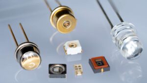

The EPIGAP OSA Photonics Group produces LED chips, SMD LEDs, TO LEDs and LED modules in chip-on-board technology in Berlin.

Our production areas
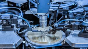
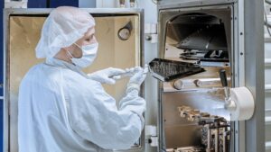
As a vertically integrated technology and production company, we offer a wide range of manufacturing technology for samples as well as small and medium batch quantities. All processes are carried out in our ISO Class 7 to 5 clean rooms in compliance with ISO 9001. Due to a close connection between the divisions, we are able to react flexibly to customer requests, e.g. in order to realize changed requirements or increases in quantities.
Starting from epiwafers of different sizes, we manufacture high quality LED chips in the wavelength range 600nm – 1100nm.
A typical process flow includes, for example:
- Material logistics, selection and procurement of raw materials and semi-finished products/wafers
- Fitting and incoming goods inspection
- Pre-selection of wafers according to desired target specification
- Metallization
- Photolithographic structuring
- Dicing
- Fully automatic final measurement and selection
Thanks to extensive documentation, we are able to trace each delivery lot back to the wafer if required. In any case, a 100% final measurement of electrical and optical parameters as well as an optical inspection is performed. Customer-specific selection criteria are possible.
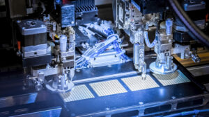
The SMD division manufactures surface mount LEDs in standard and special packages on fully automated machines. The range includes PCB-based standard components, ceramic high-power components as well as various multichip solutions. With a wavelength range offered from 255nm to 1650nm, the entire available spectrum is covered. Due to a flexible machine park, quantities from a few 100 LEDs up to several million components are possible.
Typical process steps include:
- Material logistics (raw material and component procurement, bin selection of chips)
- Incoming goods inspection and bin correlation measurement
- Automatic chip bonding (silver epoxy, AuSn solder, flip chip)
- Automatic wire bonding
- Encapsulation (silicone or epoxy encapsulation, positioning of lenses or glass caps)
- Dicing
- Automatic end measurement and binning
- Package (Tape & Reel)
Extensive documentation enables complete traceability of the chips used (down to the wafer in the case of proprietary chips). All products have a 100% final measurement of electrical and optical parameters. Customized binning even in narrow binning classes is possible.
Only customer-specific modules are manufactured in the Chip on Board production area. Due to a large technological breadth as well as the interaction of manual and automatic processes, we are able to react flexibly to your request within a short time. Production takes place in ISO Class 7 clean rooms at the Berlin site.
A selection of our technological capabilities and processes:
- Material logistics (raw material and component procurement)
- Goods receipt and pre-selection of components and bins
- Soldering process (SMD and THT assembly)
- Chip bonding (manual and automatic, flip chip)
- Wire bonding (gold and aluminum wire, manual and automatic)
- Encapsulation (hermetic sealing by means of electrode welding, potting, globtop)
- Assembly of optical components (cover glasses, filters, lenses)
- Burn-In
- Final testing and qualification
- Packaging (tape & reel, trays) and delivery logistics
The focus of module production is on OEM modules for medical technology/biophotonics, industrial applications/sensor technology and safety technology. Continuous documentation ensures traceability of the materials used. Special requirements for material selection (e.g. biocompatibility according to DIN EN ISO 10993), assembly processes or qualification and documentation (e.g. serialization with individual measurement report per module) are possible after consultation.