
Competencies
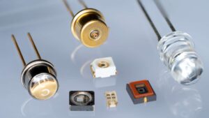
Our EPIGAP OSA Photonics GmbHdevelops and produces state-of-the-art LED chips, SMD LEDs and customized LED modules in Berlin.

Competent development services
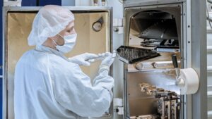
In the packaging technology sector, semiconductor chips are precisely assembled and hermetically sealed. Competent development services are combined with a deep understanding of complex manufacturing processes to take products from initial prototypes to production readiness.Our flexible in-house manufacturing in multiple ISO Class 7 to 5 cleanrooms is designed to accommodate different sized production runs. We are able to guarantee short development cycles as well as an uncomplicated series transfer. Throughout the entire process, development is geared towards cost-optimized production under the highest quality requirements.
The vertically integrated structure of the EPIGAP OSA Photonics Group enables us to optimally coordinate all components and processes along the entire value chain. In-house semiconductor manufacturing also provides more secure access to core components as well as deep subject matter expertise.
Fully monitoring along the entire value chain:

Chip Development
Development begins with the selection of the specific wafer material. Through our photolithography, we define the special contact layout and the special chip dimensions according to customer requirements.
Chip Design
The chip design defines the emitting areas. This applies equally to the chips in the high-power range and to our small display chips - miniature displays that can display any symbols and digits at the customer's request.
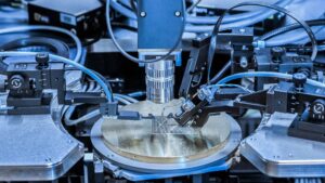
Wafer Dicing
The processed chips are separated after 100% measurement on the wafer saw. A high-speed spindle equipped with an extremely thin diamond blade is used for this purpose.
Package Selection
The perfect case fulfills several functions. It protects the chip and bonding wire, ensures efficient light extraction and optimal thermal management for reliable operation and long life.
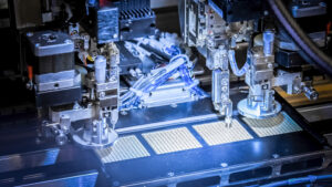
Wired Bonding
Our chips can be bonded with either gold or aluminum wire. For high power chips, multiple bonds ensure efficient operation at high currents.
Encapsulation
The potting makes a significant contribution to efficient light extraction. We use epoxy or silicone depending on the wavelength range and application.
Black potting materials can also be used for special beam forming requirements.
Lens Assembly
The beam shaping of the light can be decisively influenced by the use of a lens. That is why SMDs with lens are one of our standard products. In addition, glass lenses or lens arrays can be used for customized products.
- Semiconductor chip design, module design, optics simulation, mechanical design and supply logistics
- LED chip prototyping
- Prototyping of optoelectronic components, modules and assemblies
- Test and qualification
- Series production
Our own production in Germany enables us to deliver customer-specific products in consistent quality for years.
